Problem Statement:
You have two (or more) STM32 Nucleo boards, and need their clocks to be synchronized. This means, that we allow for a non-zero phase offset between the clocks, but the phase offset should not change with time.
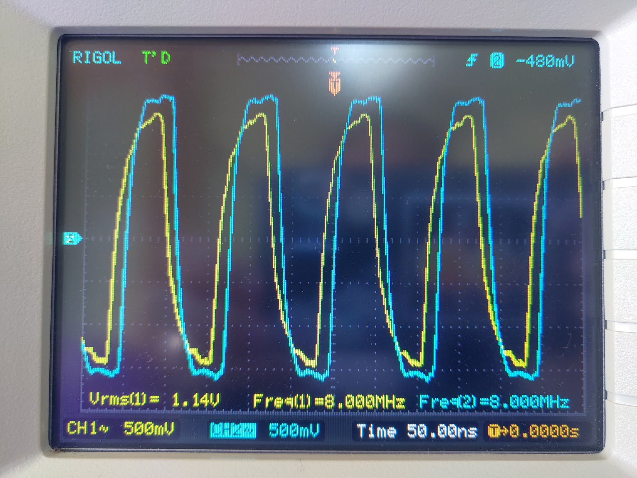
One way to confirm this is that viewing the clock outputs for the two boards on your scope, triggering off one waveform should freeze the other clock waveform too.
Solution:
1. Setting up the clock on the MASTER board:
a) within STM32CubeMX navigate to the "System Core" -> RCC tab and set the LSE clock source to "Crystal/Ceramic Resonator". Also, check the "Master Clock Output" checkbox. Doing this will send the clock to the MCO pin on the board (usually GPIO pin PA8). You will then connect that pin on the MASTER board to the CN7pin29 on the SLAVE board. See figure 1 for an example.

Note: The MCO pin likely automatically be configured as "Alternate Function Push Pull", however, in addition, you will need to set the maximum output speed for this pin to "High" (the default is "Low").
b) open STM32CubeMX for your slave board, and navigate to the "Clock Configuration" tab to see the acceptable external HSE input frequency range. Then locate the "MCO Source Mux" in STM32CubeMX of the MASTER board and select the MCO frequency to be within this range (usually 1 - 32 MHz). See figure 2 for an example clock configuration on the MASTER board.

c) program the board. Hook up a scope MCO output (GPIO pin PA8) of the MASTER board, and confirm that you get a clock signal of the appropriate frequency. See figure 3.

2. Setting up the clock on the SLAVE board (the same configuration may be repeated on other slave boards):
a) refer to the User Manual for your board and understand what board configuration is required to configure the external high-speed clock (HSE) pins to accept input from an external oscillator through pin CN7pin29 (i.e. PF0 pin). In my case both boards are MB1136, and suggested configuration on page 24 is shown in figure 4.

Note: Make sure to get the correct manual; look up the MB number at the back of the Nucleo board and get the manual for that numbered board. In my case the MB number for both boards is MB1136, and hence this is the appropriate manual.
b) within STM32CubeMX navigate to the "System Core" -> RCC tab and set both HSE/LSE clock sources to "BYPASS Clock Source", see figure 2. Checking the "Master Clock Output" checkbox is not necessary, but will help verify that you have in fact synchronized the clocks at the end of this exercise.
Note: The Master Clock Output (MCO) is usually output to GPIO pin PA8 on most (but not all STM32) boards. This GPIO pin will automatically be configured as "Alternate Function Push Pull" but in order to see an output on the scope the maximum output speed for this pin should be set to "High" (the default is "Low").
c) figure 5 provides the clock diagram for the slave board. Program the board.

3. Putting it all together:
a) connect the MCO output of the MASTER board (GPIO pin PA8, CN12pin23) to the expected HSE clock input pin on the SLAVE board (GPIO pin PF0, CN11pin29).
b) connect a scope to the MCO outputs on both the MASTER and SLAVE boards to confirm that the clocks are in sync. See figure 6.